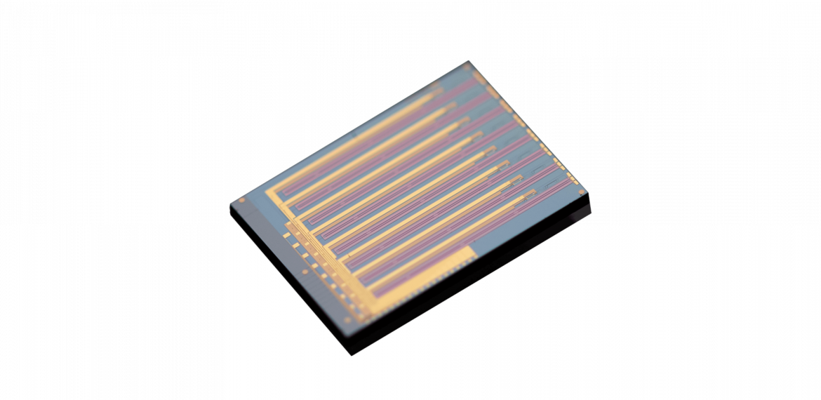
Global data centers are currently navigating a hardware transition where electrical interconnects can no longer keep pace with the massive throughput required by artificial intelligence. To solve this bottleneck, the industry has turned toward photonic chips, which utilize light particles instead of electrons to transmit and process information. By moving data through optical waveguides, these chips drastically reduce heat generation and signal degradation over distance. This shift is particularly evident in the development of 3.2T DR8 solutions, where the integration of advanced TFLN chips allows for unprecedented speeds. These thin-film lithium niobate components provide a foundation for managing the 400G-per-lane signaling that defines the next decade of high-speed digital infrastructure.
The Architecture of Next-Generation Photonic Chips
The fundamental purpose of photonic chips is to manipulate light with the same level of precision that traditional processors apply to electricity. Within these integrated circuits, components like lasers, detectors, and modulators are miniaturized onto a single substrate. For B2B infrastructure, the efficiency of these modules is measured by their ability to maintain high signal-to-noise ratios while reducing the physical footprint of the transceiver. As per-lane speeds reach toward 1.6T and beyond, the reliance on specialized TFLN chips has become essential for achieving the bandwidth necessary to support modern hyperscale workloads without a proportional increase in energy consumption.
Performance Breakthroughs with TFLN Chips
The physical properties of thin-film lithium niobate represent a significant advancement over traditional silicon photonics. Modern TFLN chips offer a 3dB-bandwidth of 110GHz and beyond, which is critical for the ultra-fast switching required in 3.2T networks. Furthermore, these components achieve a half-wave voltage of less than 1.5V, allowing them to operate at significantly lower power levels. By integrating such high-performance photonic chips into the system, designers can achieve an insertion loss of less than 14 dB even when accounting for coupling loss. This high level of efficiency ensures that optical signals remain strong across complex network fabrics, supporting mid- to long-reach telecom solutions.
Industrial Applications in 3.2T Networking
Scaling to a 3.2T DR8 optical module requires hardware that can handle 8 channels of 400G data simultaneously. In this context, the use of TFLN chips provides the necessary DC-ER of over 25 dB to ensure clear signal differentiation. These photonic chips support both differential and single-ended coupling, offering the flexibility required for diverse system-level solutions in automobiles, instruments, and communication networks. Because these designs are capable of mass production, they offer a commercially viable path for high-tech enterprises to deploy next-generation PICs in everything from coherent optical systems to FMCW Lidar sensors for autonomous driving.
Conclusion
The evolution of the information and communications sector is increasingly dependent on the precision of light-based hardware. Through the development of high-speed, low-loss modulation devices, the industry can successfully navigate the complexities of 3.2T architectures. High-tech enterprises like Liobate are central to this progress, providing the specialized TFLN modulator chips and sub-assemblies needed to drive high-capacity optical modules. By establishing advanced platforms for PIC design, fabrication, and packaging, Liobate ensures that customers have access to the superior products and services required to scale bandwidth globally. As Liobate continues to refine its thin-film electro-optic technology, it remains a key contributor to the advancement of sustainable, high-speed connectivity.


